Saturday, October 13, 2018


Full Adder


Hello friends today we are going to learn about full adders and we will also use labVIEW to complete our task 2.

To make my post even more interesting I use other software such as MATLAB ,pspice ,NI Multisim.

In my previous post we discussed about half adders and we also used programming software such as pspice , MATLAB , labVIEW , NI Multisim.

I hope you are clear with a half adder circuit and there working. One thing keep in your mind that binary addition is different from normal decimal addition.

Let’s get started

What is a full adder?

A full adder is similar to that of an half adder but full adders are capable of adding 2 one bit binary number along with a carry, were as half adder we can only add 2 one bit binary number.

How to construct a full adder circuit.

A full adder circuit is very simple if u ask me I will say it’s the simplest one.
When 2 half adder circuit is connected together we get a full adder circuit.


And we already know that the half adder circuit uses EXCLUSIVE-OR GATE, and AND GATE.


And for full adder we need 2 EXCLUSIVE-OR GATE,2 AND GATE and one OR gate.


For a full adder circuit we have 3 input and 2 output.


STEP 1:

Connect pin A and pin B parallel with EX-OR and AND gate to construct half adder 1. Similarly do the same for half adder 2

STEP 2:

Take the output of EX-OR gate from HALF ADDER 1 and connect as one of the input to half adder 2

STEP 3:

An additional input terminal C which is the carry in pin connect it with half adder 2

STEP 4:

Now we have 3 output pins but we need 2 pins output sum and carry out
Use OR GATE and connect output of AND GATE from half adder 1 and half adder 2. The output of OR gate is the carry out for the full adder circuit and EX-OR gate is the sum.
So now we are clear how to design a half adder circuit let’s see how to implement the same with the help of software such as pspice, MATLAB , labVIEW ,and  NI Multisim.


LABVIEW

STEP 1:

Open LABVIEW software


STEP 2:

Press ctrl + N to open a blank .vi


STEP 3:

For multitasking press ctrl + T to access front panel and block diagram window at the same time.


STEP 4:

Use Boolean functions from function palette.


STEP 5:

Place the logic gates as per your requirement.

STEP 6:

Make your connections properly and your program is ready.

STEP 7:

Run your program and your output is ready.


PSPICE


STEP 1:

Open Pspice (capture CIS) software


STEP 2:

Go to file-new-project


Now you get 4 options


1 : Analog/mixed A/D
2 : Pc board wizard
3 : Programmable logic wizard
4 : Schematic

STEP 4:

Choose Analog/mixed A/D because we are working with digital circuits.
If you are installing for the first time then you have to specify the path where to save the files.

STEP 5:

Now a pop up window appears "create pspice project window" choose "create a blank project”.


STEP 6:

Now you are to ready to program your select the components from library.


STEP 7:

After making finishing the full adder circuit you’re are ready to simulate.


MATLAB


STEP 1:

Open Matlab software


STEP 2:

Go to new simulink model.


STEP 3:

Wait for a while once Simulink model window appears select “library browser” form toolbar.

STEP 4:

Under library toolbar select go to Simulink-logic and bit operation.(This window will help you to add logical functions for the blank .mat file)


STEP 5:

Add constants for input from Simulink - sources

STEP 6:

Add display for viewing output from Simulink - sinks.

STEP 7:

After completing your program run the program and your output is ready.


NI MULTISIM


STEP 1:

Open NI Multisim

STEP 2:
As soon as you open multisim you can start your simulation.

STEP 3:

The toolbar contains all basic components such as resistor, diode, transistor etc.

STEP 4:

Once you click any components such as resistor library window appears on the screen.
With the help of the library files you can places thousands of different components.


STEP 5:

Multisim simulation is similar to that of practical experiments you have to place led for output switches for input and other components such as multimeter, CRO for output.

STEP 6:
After completing your circuit you have to click the play button which appears on top of the screen.


LabView Full adder basic file


LabView Full adder  file


PSpice Full adder file


NI Multisim Full adder file


DOWNLOAD


MATLAB Full adder Simulink file


What’s next?

 In my next post we are going to learn about RS-Flipflop
If you like my post like share and subscribe to my youtube channel "ANK LABS".
Support me on blogger and google+.


Saturday, September 8, 2018


ANK LABS
HALF ADDER


Hello friends today we are going to learn what is a half adder? & how they work, To make my post Even more interesting I used simulation software such as LABVIEW, PSpice, NI Multisim etc. These simulation software provides a realistic environment and it make learning Even more interesting.


HALF ADDER

v A Half Adder adds two one bit binary number.


v A binary number is understood by machines. And they have only two symbol 0 (zero) & 1 (one).

v Have a look at this table which shows the binary equivalent of decimal number. (4 bit binary number).


v To perform addition using half adder, use 2 one bit binary numbers.
A & B

v Before performing our addition program let’s do it manually.

binary addition is similar to that of normal decimal addition 
when A and B are zero we get zero, when A is zero and B is one the output is 1, but in case when both A and B is 1 the output is 1 0 but for decimal addition it is 2 .


A     0            0             1

                   B     0            1             1                 2

                            0            1          1  0              1 0


LabView – for labview simulation I used one AND gate, one EX-OR gate along with controls and indicator.


In front pannel window i used AND & EX-OR gate to design a half adder circuit.


PSpice – for PSpice I used AND and EX-OR gate from components library and connected with there respective devices.


NI Multisim – for Multisim I used AND and EX-OR gate from components library and connected to respective devices.


 Additionally I connected a CRO which allowed me to visualize the waveform, These is a  HIGH and LOW signal which determine ON and OFF condition of gates.


MATLAB – In MATLAB I used Simulink model and AND & XOR gate to perform our logical operation.


You can download simulation files you can also make use of truth table to have a better understanding. I have also added a power point presentation which you can download.


LabView Half adder file


LabView Half adder simulation file


PSpice Half adder file


NI Multisim Half adder file


DOWNLOAD


MATLAB half adder Simulink file


PPT file free download


If you still have problem in understanding any of this concept you can visit my YouTube channel     “ANK labs” 


Saturday, August 4, 2018

 ANK LABS 
  
LOGIC GATES

Hello friends today in this Post I will explain each and every functions in Boolean control palette. if we compare functions in Boolean palette with logic gates there are same, That means we can perform all operations with can be done with logic gates well logic gates can be used for binary addition, binary subtraction and much more.
After finishing our tutorial I will give some example task for you. If you find difficult I will explain later in my upcoming video you can easily finish the task if you understand carefully. Have fun.

In this tutorial we will be covering the following functions under Boolean palette.
Add caption


Let’s get started:
AND gate
The AND gate gives a high output (1) only if all its inputs are high.  A dot (.) is used to show the AND operation you can consider the same as A.B but it’s should be denoted as AB.


OR gate
   The OR gate is an electronic circuit that gives a high output (1) if one or more of its inputs are high.  A plus (+) is used to show the OR operation. It’s just simple as adding  (0 and 1).but of course 1+1 is not 2 in this case logic's can have only two values either high that is (1) or low that is (0)


NOT gate

                The NOT gate produces an inverted version of the input at its output. They are also called as inverters. If the given input is HIGH the corresponding output will be LOW.


NAND gate
                This is a NAND gate which is equal to an AND gate followed by a NOT gate. The outputs of all NAND gates are high if any of the inputs are low. If you see this image its similar to an AND gate but has a circle at the output this small circle is called the inversion.

The output of NAND gate is the same as AND gate but the output is inverted


NOR gate
                This is a NOR gate which is equal to an OR gate followed by a NOT gate. The outputs of all NOR gates are LOW if any of the inputs are HIGH. If you see this image its similar to an OR gate but has a circle at the output this small circle is called the inversion.


EX-OR gate


The EX-OR gate which is 'Exclusive-OR' gate give a high output if either, but not both, of its two input are high. The EX-OR gate is denoted by an encircled plus sign .


EX-NOR gate

   The EX-NOR gate which is 'Exclusive-NOR' gate which give a low output if either, but not both, of its two inputs are high.


The NAND and NOR gates are called universal gates because they can perform the operations of all basic logic gates such as AND, OR and NOT gates.

This simulation can also be done in labVIEW . The programs which you create in labVIEW can also be used as standalone application. labVIEW run time engine help us to use them without labview software.

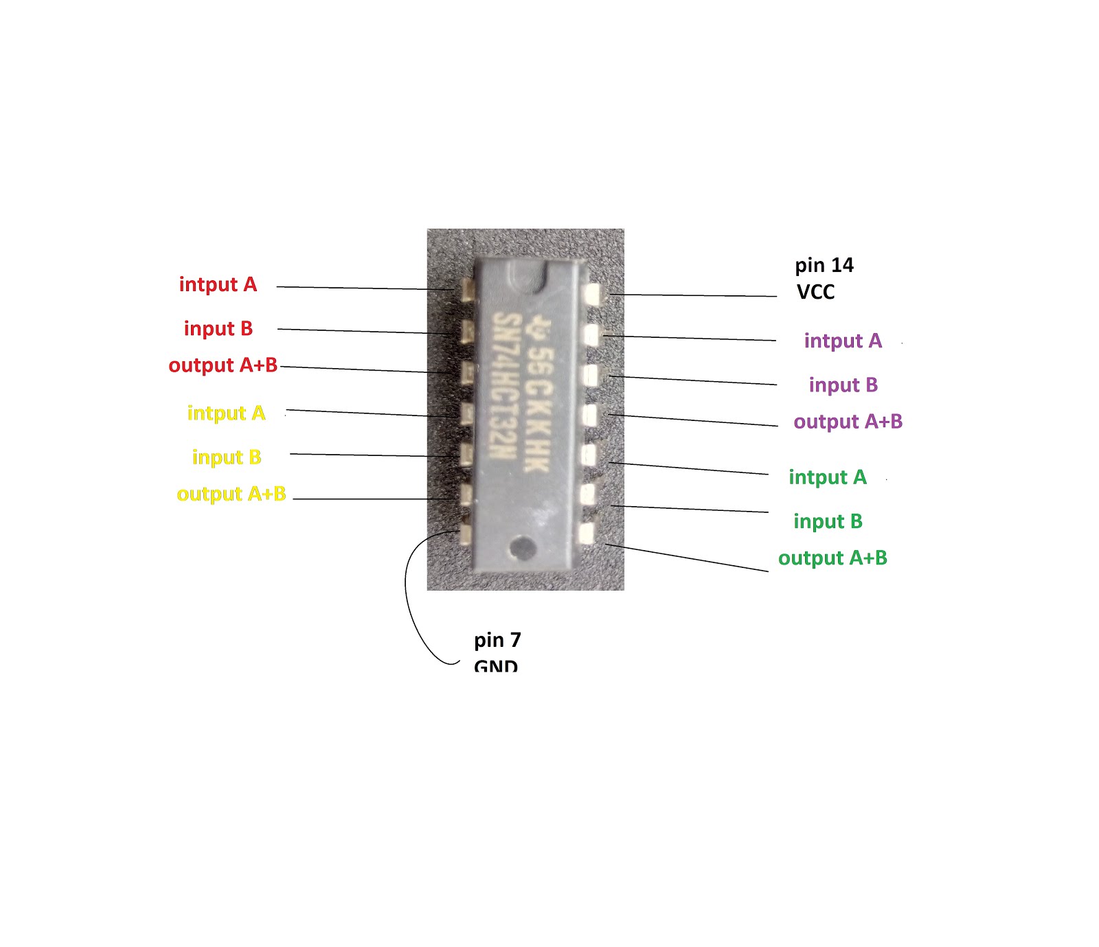
What will you do if someone ask you to realize the logic gate using IC’s, well you can perform all that you want using the logic gate IC’s I would have made a separate post on that due to time shortage and it’s a boring topic so I quit. But I can do one thing I can teach how to use wire them.
Download data sheet for more details.

AND gate

3 input AND gate

OR gate

NOT gate

NOR gate

IMAGE NOT AVAILABLE

NAND gate

EX-OR gate


This tutorial ends here the same content will be uploaded in my youtube channel so don’t Forget to like share and subscribe.

 Follow my blog for more updates.

LabView task:
1 - HALF ADDER USING LABVIEW BOOLEAN 
     DATA TYPE.
2 - FULL ADDER USING LABVIEW BOOLEAN 
     DATA TYPE.                          
3 - RS FLIP-FLOP USING LABVIEW BOOLEAN 
     DATA TYPE.
4 - JK FLIP-FLOP USING LABVIEW BOOLEAN 
      DATA TYPE.
5 - GLOW FIVE LED'S WITH DIFFERENT COLOR 
      USE ONE BOOLEAN CONTROL.

labVIEW logic gate Simulation
Don’t forget to use my simulation programs.

AND GATE


OR GATE


NOT GATE


EXCLUSIVE-OR GATE


NOT EXCLUSIVE-OR GATE


NOR GATE


NAND GATE


DOWNLOAD .vi file


DOWNLOAD .vi file (SIMULATION)


What’s next?

          In my next blog/youtube video I will explain the functions of numeric control palette. Before that we will finish out 5 task under Boolean data types. This task will be explained in my youtube channel “ANK LABS”.